Home
Curo l’auto
Guide e consigli
Per Lei
Noleggio a lungo termine
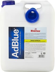
AdBlue Scontato!
Addittivo AdBlue
Parti di Ricambio
Oli e liquidi
Cerchioni e Pneumatici
Pulizia e Cura Auto e Moto
Verniciatura
Accessori per Auto
Attrezzi per Veicoli e Officina
Elettronica per Auto e Moto
Moto, Accessori e Componenti
Articoli Regalo e Merchandising
Accessori e Parti per Camper
Accessori per Viaggio e Trasporto